Successful Assembly!
I finally tracked down some sticky issues with the PCB prototype of my Ifos project. Until now, I had assumed hardware problems accounted for its non-function.
In a way, that was true, but in another more important way, it was software. I made some subtle changes in port assignments for the PCB version, then forgot to tell myself about them.
First, some background
The device uses SPI for communication between the micro-controller, dedicated LED drivers, and Flash memory. All these chips share a common SPI bus, but the μC (as the SPI master) only talks to one at a time. To pick which one, it pulls that chip’s CS (Chip Select) pin low.
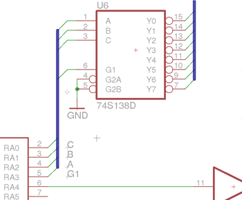
Now rather than dedicate a separate μC I/O pin to each and every CS, I use a 3-to-8 multiplexer to select one of eight using only three I/O pins. Normally, all multiplexer outputs are high, but when enabled, it reads the 3-bit number at its inputs and drives the corresponding output low. Presto! Dial in the id of the target chip and it gets “selected” to listen on the bus.
Problem 1
Specifying the chip id is straightforward, except for the fact that I reversed input pins. I/O pins RA0, RA1, and RA2 used to be connected straight-through to the multiplexer’s A, B, and C inputs, but to save an extra via on the PCB, I swapped RA0 and RA2. (Made sense at the time.) This is actually harmless for half the possible ids—0, 2, 5, and 7 are palindromic binary numbers—but the other half appear backwards, so of course the corresponding chips don’t get selected when you expect them to.

Problem 2
Recall that SPI uses active-low for chip-select (as clearly indicated by the little line thingy above the signal name, CS), and that the multiplexer will bring one of its output pins low when enabled. Unfortunately, I wired RA3 to the G1 enable, an active-_high_ input. This means that every time I want to select an SPI chip, I have to remember to use opposite logic. Bummer. I could have used G2A or G2B instead and preserved the expected behavior.
Problem 3
The SPI code had been using RC2 throughout for CS control, instead of RA3. So, not only was the logic wrong, I wasn’t even asserting the correct pin. D’oh.
Problem 4
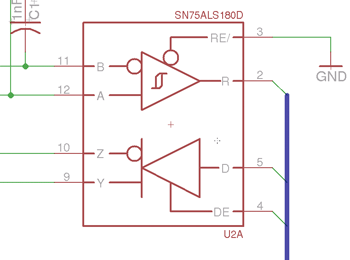
Likewise for the RS485 tranceiver, the code assumed RA3 controlled the driver enable, while the board devotes RC0 to that purpose. As we know from Problem 3, however, RA3 actually does control something: the SPI chip-select. What a coincidence. On top of everything else, the device couldn’t even communicate with the outside world, since the driver enable obviously wasn’t working either.

Success!
None of these issues affected the breadboarded prototypes since their wiring dictated the details of the software to begin with. I know what happened: I got the prototypes working, then weeks later sat down to do the PCB layout… Here or there a minor change would simplify a trace, or bring related signals to the same side of the micro-controller, so why not? Of course, I should have updated the software right then, or at least made a note to myself. Oh well.
As the title says, though, the assembled board actually works! Once I corrected all the problems above in software, it started accepting commands, lighting LEDs, and issuing responses. Finally… The board itself looks a little… lived in (cut traces, extra components, repaired traces, jumper wires, etc.), but it works like a champ.
Once the board was actually running, I did find a solder bridge on the second MAX6957 (one of the LED drivers). That made for some interesting effects. Even more dramatic, though, was one last software glitch: four entries in the LED-to-port mapping table were off, which cascaded through the port-to-pin mapping table. Lots of seemingly random LED interconnectedness. Neat!